ASML is one of the world’s leading manufacturers of chip-making equipment.
Our vision is to enable affordable microelectronics that improve the quality of life. To achieve this, our mission is to invent, develop, manufacture and service advanced technology for high-tech lithography, metrology and software solutions for the semiconductor industry.
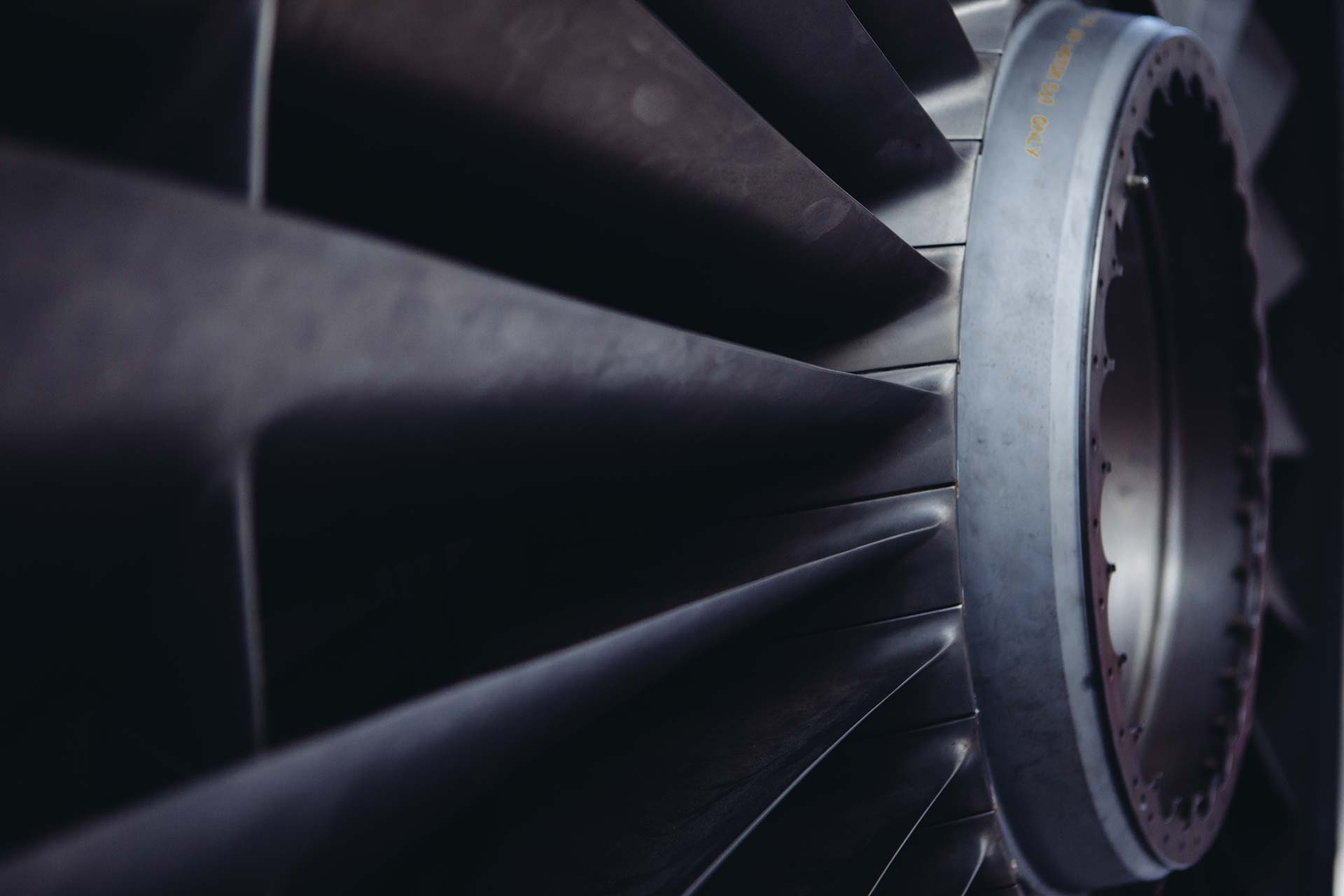
ASML's guiding principle is continuing Moore's Law towards ever smaller, cheaper, more powerful and energy-efficient semiconductors. This results in increasingly powerful and capable electronics that enable the world to progress within a multitude of fields, including healthcare, technology, communications, energy, mobility, and entertainment.
Working at ASML
We provide the world’s top chipmakers everything they need to create better performing, cheaper semiconductor chips. Simply put: we are an industry leader supporting industry leaders.
As such, you’ll be encouraged to bring your best ideas and act on them. You’ll have the freedom, trust, and support in your field to experiment and solve complex challenges. Things are rarely dull when you’re constantly breaking new ground.
But despite our fast-paced environment at the forefront of tech, we take your work-life balance and wellbeing seriously. A business is only as good as its employees.
So join us, and you’ll be a part of a global collaboration. One that promotes creativity, the inclusion of highly diverse teams, and an exciting and dynamic work environment. Join us, and you’ll be a part of progress.
Introduction
Are you our new skilled and creative brain who goes the extra mile to solve challenging technical puzzles related to our clamp qualification and test equipment? If so, we are looking for you!
Job Mission
As a test development engineer in the EUV wafer clamping group you will be part of our electrostatics team. Within this team, very specialized test equipment is maintained, improved and developed. With these experimental test setups we improve our understanding of how clamps truly work and we can qualify new designs. These setups are complex, state-of-the-art vacuum test setups packed with intelligent sensors and mechatronic systems to measure crucial characteristics of our wafer clamps.
Your in depth knowledge on vacuum hardware technology and software that controls this hardware together with your drive to continuously improve makes you an indispensable player in our team.
Job Description
As a test development engineer for electrostatic wafer clamping you :
Education
Bachelor or Master in Electronics, Applied Physics, Mechanical Engineering, Optics or Biomedical Engineering.
Experience
Other information
We offer you a position in a team that consists of skilled, motivated people that have a passion for technology. At ASML we push capabilities of our technology to the level that is considered to be impossible by external experts. We also have a huge drive to truly understand what’s physically happening on the nanometer scale that we are examining. Though we stay pragmatic as our customers need real solutions, not just theories. Do you see yourself in this picture
| Education Backgrounds: |
Business Engineering |
| Specialties: |
Other Research (R&D) Testing |
| Education Level: |
Undergraduate (Bachelors) |
| Experience: |
2 - 5 years 5 - 10 Years |
| Languages spoken: |
English |
| Job Location: | Veldhoven, Netherlands |
To apply for this position you will be taken to the recruiter's website. Please click Next below to continue.
Next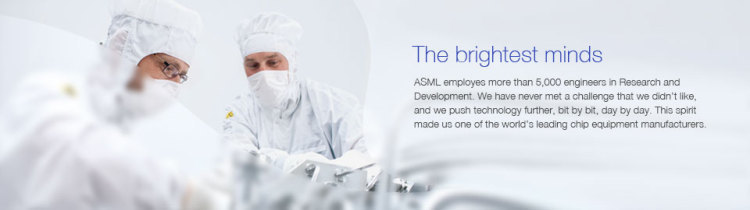

Type: Job
Deadline: 15th June 2025
Job reference (ID): 18217

Loading...